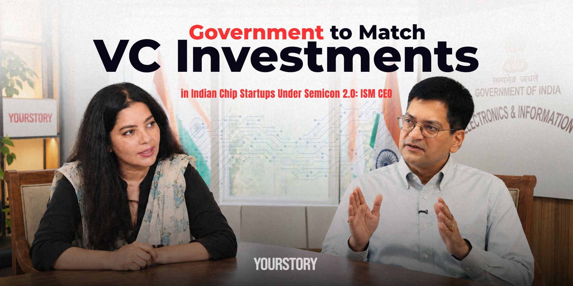
When the government backs a chip startup and it gets acquired, is that a failure? Amitesh Kumar Sinha, Additional Secretary at the Ministry of Electronics and Information Technology and CEO of the India Semiconductor Mission, has a ready answer: not necessarily. It can also be a return on investment. That distinction is becoming more important as India enters the next phase of its semiconductor push. Indian semiconductor companies have attracted $1.4 billion in cumulative equity funding, with $701 million, nearly half the total, raised since 2025, according to Tracxn data. Now the government wants to bring more private capital into chip design by investing alongside venture capital firms.
Speaking to Shradha Sharma, Founder and CEO of YourStory and The Bharat Project, days before Semicon India 2026 opens in New Delhi, Sinha laid out the thinking behind Semicon 2.0, the second phase of the mission that turns the government from grant-giver into co-investor, including a model under which the government will match VC investments in approved chip startups rupee for rupee on the same terms.
"Seed funds for startups are grants; the rest is our investment, so the government shares both the upside and the failures," he said.
A mission that has kept its schedule
When YourStory last spoke to Sinha ahead of Semicon India 2025, the India Semiconductor Mission had 10 approved projects and design tools rolled out to 280 colleges. A year on, the count stands at 12 manufacturing units with a cumulative committed investment of over Rs 1.64 lakh crore: one silicon fab, one silicon carbide fab, an integrated gallium nitride micro LED display fab and nine packaging units. Three of the 12, Micron, Kaynes and CG Semi, have started commercial production, all in Sanand, Gujarat. On the design side, 24 startups have been approved for support, and Sinha said 15 of them have raised venture funding.
That first phase, which began implementation in 2022 under a Rs 76,000 crore outlay, is what he calls Semicon 1.0. The Union Cabinet approved Semicon 2.0 on 15 July 2026 with an outlay of Rs 1,27,500 crore, and MeitY notified the scheme on 31 August 2026. It is built on six pillars: design, equipment and materials, fabs, advanced packaging, research and development, and talent.
"Semicon 2.0 arriving on time proves it," Sinha said of the long-term commitment made by the Prime Minister and Union Minister Ashwini Vaishnaw.
Why the second phase looks different
Phase one, in Sinha's telling, was about anchoring demand. The 12 approved projects told the government what they needed from a supply chain, and that exposed the gap. "When your industry is still small, supply chain partners prefer to export to India rather than move here," he said. Only bulk essentials set up next to a factory.
Semicon 2.0 is meant to close that gap. Equipment accounts for around 65% of the cost of a manufacturing plant, he explained, and chemicals, gases and materials make up about half of running costs. Getting those suppliers to set up in India is how the cost of manufacturing comes down and Indian companies become competitive.
The timing, he argued, is also on India's side. With the global semiconductor industry expected to expand sharply over the coming years, manufacturers and suppliers will have to add capacity somewhere. India's bet is that a growing domestic market, government incentives and an emerging manufacturing base can persuade more of that supply chain to move here.
The change that matters most, though, is in design.
How does the government's co-investment model for chip startups work
Under the first phase, the design scheme offered startups and MSMEs seed funding and access to electronic design automation tools, which are prohibitively expensive for a small team. The trouble came after proof of concept. A chip takes another one and a half to two and a half years to design depending on complexity, Sinha said, and that costs money the scheme did not cover. A single chip design can run from Rs 25 crore to Rs 35 crore at the simpler end to Rs 1,000 crore to Rs 2,000 crore for complex parts.
Semicon 2.0 adds a co-investment layer. After seed funding, if a venture capital firm invests in an approved startup, the government puts in an equal amount as an investor on the same terms. Large Indian companies that may not want to give up equity can opt for royalty-based funding instead, again matched rupee for rupee. Exit paths follow industry practice, and any company can exit when it chooses.
The intent is to pull VCs into a sector they have largely avoided. "In Silicon Valley, Israel, wherever design companies flourish, VCs invest, understand the business, mentor startups and help with market access," Sinha said. And he is prepared for the political question that follows when a state-backed startup is bought by a foreign company. "If we try to control it, the ecosystem will not form," he said. A founder who is acquired comes back with capital and experience, tries again, and after one or two attempts builds the company the mission actually wants, an Indian fabless firm with its own IP. If a startup is acquired, the government takes its share according to its equity stake, exactly like any other investor, and uses that money to fund the next one. In other words, Semicon 2.0 is not designed to prevent exits. It is intended to create a cycle in which successful exits return capital and experience to the ecosystem.
The self-reliance clock
Shradha asked how much of India's chip demand domestic capacity will meet, and by when. Sinha gave a segment-by-segment answer rather than a single date. In packaging, he expects India to cover domestic demand and export in large volumes within five to six years, moving into a leadership role in advanced packaging. Even then, 10% to 25% of unique, advanced chips will still be imported because their plants are not here.
In fabrication, Tata's Dholera plant covers nodes from 28 nanometre to 110 nanometre, and he expects full capability above 28 nanometre to follow, with more compound semiconductor fabs under Semicon 2.0. On a 10-year view, he said, India will be self-reliant in legacy chips and begin exporting them once its own requirement is met. Cutting-edge chips at 2 nanometre and below may continue to be imported. "This could take 10 to 12 years," he said.
Shradha's closing question set a 10-year horizon: what must have happened by 2035 for him to call the mission game-changing? His benchmark was specific. Self-reliance in legacy fabs and every kind of packaging, with large export volumes, is the baseline. If India has closed the gap at the cutting edge by then, "I will call that success." If it has begun working in parallel with the leading edge, "I will call it super success."
India's semiconductor market was valued at 45 billion dollars to 50 billion dollars in 2024-25 and is expected to reach 100 billion dollars to 110 billion dollars by 2030, according to PIB.
Where the jobs are, and who is filling them
Shradha put the question the way a student in Patna, Indore, Bhubaneswar, Coimbatore or Kochi might: is this industry only for Tata and IIT startups? Sinha's pitch started with design, which he says accounts for roughly 50% of the semiconductor value chain, with 20% of the world's design engineers already Indian. The Chips to Startup programme provides costly design tools free to more than 300 colleges, according to PIB, and student designs are fabricated at the Semiconductor Laboratory in Mohali, packaged and sent back. "A student who has seen one full cycle leaves college as a confident design engineer," he said.
The Design Linked Incentive scheme, he added, is drawing back Indians with 25 to 30 years of design experience abroad who now want to set up ventures at home. A chip design company employs 50 to 200 people, and if it scales, "it becomes Qualcomm, which employs 20,000 engineers in India." Beyond design, he listed chemical, materials, civil and mechanical engineering as streams a fab depends on, and cited an industry multiplier of around 5.7 for jobs created beyond the plant.
His most striking example was prompted by Shradha's observation that deep tech conversations often leave women out of the picture. At CG Power's plant in Sanand, the operators working on semiconductor equipment and packaging chips are all women, drawn from Jharkhand, Madhya Pradesh, Bihar, Odisha and the North East, with what he called ordinary education and no prior exposure to the industry. They were sent to Malaysia for training, the first time most had left their home towns. "Meet them today and they will explain chip packaging to you like confident engineers," he said. Women already make up more than half the electronics workforce, and in some factories all of it, he noted, and he expects semiconductors to follow. Semicon India 2026 will carry a dedicated session on women in the industry, with senior Indian women leaders of global chip firms speaking to students.
Semicon India 2026 by the numbers
Semicon India 2026 runs from 17 to 19 September 2026 at Yashobhoomi in Dwarka, New Delhi, with Prime Minister Narendra Modi inaugurating it on 17 September and holding his annual Country Round Table with global CEOs on 16 September. Sinha said more than 575 companies are participating, up from 350 last year, of which around 300 are international and 86 of those have an India headquarters. Participation has grown to more than 50 countries and seven country pavilions, and he said 12 states are taking part. SEMI, which declined to hold the conference in India in 2022 and 2023 for want of an industry, has partnered with ISM and IESA since 2024.
New this year is a Workforce Development pavilion inside the exhibition, with student mentorship, training on the full fab process, a day-long session run by experts from Singapore on 18 September and company-funded hackathons. A Semicon India 2026 mobile app offers venue navigation, session schedules and consent-based AI matchmaking with bookable meeting rooms. Main sessions will be webcast for those who cannot travel to Delhi.
The mission's own scorecard
By the metric the mission uses, a design startup becomes a unicorn at 1 billion dollars in revenue. "Many unicorns is what we want to see in semiconductor design," Sinha said. That, alongside export volumes from legacy fabs and packaging plants, is how he wants the mission judged in 2035.
The nearer test is quieter. Order negotiations with large global companies for the plants now entering commercial production are at an advanced stage, he said, with some ready to book entire facilities and already discussing expansions at plants not yet built. If those orders land over the next year, they will offer an early indication of whether India's semiconductor push is moving beyond government-backed capacity creation towards a commercially sustainable industry. And by Semicon India 2027, the mission could be measured against a very different baseline from the one it is setting this September.
Source: YourStory